Material science and technology of nanomaterials of nanosystems. Nanotechnology, materials science and mechanics
Recommended for publication by the Institute of Metallurgy and Materials Science (IMET) im. A.A. Baykov RAS (Laboratory of Physical Chemistry and Coating Technology - Head of Laboratory V.I. Kalita, Doctor of Technical Sciences, Professor) and St. Petersburg University of Engineering and Economics (Department of Engineering and Technical Sciences - Head of Department V.K. Fedyukin, Doctor of Technical Sciences, Professor, Corresponding Member of the International Academy of Higher Education) as a teaching aid for university students studying in technological areas of training as part of the course "Modern technologies and materials for industries."
Received the UMO Graph for PPO No. 04-01 (Approved by the Educational and Methodological Association for Vocational Pedagogical Education as a teaching aid for students of higher educational institutions).
Scientific and technological progress in the field of high technologies - in materials science, electronics, micromechanics, medicine and other areas of human activity is associated with the results of fundamental and applied research, design and practical use of structures, materials and devices, the elements of which have dimensions in the nanometer range (1 nm = 10-9m), and the development of technologies for their manufacture (nanotechnology) and diagnostic methods. The objects of nanotechnology in materials science are dispersed materials, films and nanocrystalline materials.
The purpose of the manual is to familiarize students and specialists with a new effective direction in the development of science and technology in the field of nanomaterials and nanotechnologies, in particular, the synthesis of nanocrystalline structural materials with unique properties and examples of their use in industry.
The manual discusses the theoretical and technological foundations, problems and prospects of nanoscience and nanoindustry. Definitions of the basic concepts of nanoscience are proposed. The data on nanomaterials and nanostructures are systematized and their classification is given. Methods for research and design of nanostructures are described. An analysis is given of methods for the synthesis of nanostructured materials and a number of examples of their application in traditional and new technologies in various industries. The features of changes in the physical, mechanical and technological properties of structural and functional nanomaterials are considered.
The textbook is designed for students of higher educational institutions studying in various specialties, studying courses in materials science and technology of structural materials. It may be useful for graduate students, specialists and researchers dealing with nanomaterials and nanotechnologies.
The structure of the tutorial:
Introduction.
Chapter 1. Fundamentals and aspects of the development of the science of nanomaterials and nanotechnologies.
Chapter 2. Nanomaterials and nanostructures.
Chapter 3. Methods for studying and designing nanostructures.
Chapter 4. Technologies for obtaining nanostructured materials and manufacturing nanoproducts.
Chapter 5. Mechanical properties of nanomaterials.
Conclusion.
Bibliographic list.
List of terms.
Appendix: Specialized Exhibition of Nanotechnologies and Nanomaterials.
Bibliographic link
Zabelin S.F., Alymova M.I. MATERIAL SCIENCE AND TECHNOLOGY OF NANOSTRUCTURED MATERIALS (TUTORIAL) // International Journal of Experimental Education. - 2015. - No. 1. - P. 65-66;URL: http://expeducation.ru/ru/article/view?id=6342 (date of access: 09/17/2019). We bring to your attention the journals published by the publishing house "Academy of Natural History"
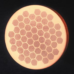
Carbon nanotube model
The end of one year and the beginning of the next is a special time when humanity is visited by the desire to analyze the past and reflect on what lies ahead. And at the beginning of the new year, we want to review the 10 most important achievements in nanotechnology since the beginning of their development, related to materials science.
This is how J.Wood, one of its editors, begins his publication in the post-New Year issue of Materials Today, wondering what events of the past 50 years have determined today's high dynamics in the development of materials science. Wood identifies 10 events (not including the discovery of high-temperature superconductivity here, obviously as an event more significant for physicists than for materials scientists).
At the first place- "International Technology Roadmap for Semiconductors" (International Technology Roadmap for Semiconductors - ITRS), not a scientific discovery, but, in fact, a document (analytical review) compiled by a large international group of experts (in 1994, more than 400 technologists were involved in compiling the Map, and in 2007 more than 1200 specialists from industry, national laboratories and academic institutions). Combining science, technology and economics, the Map sets out goals that can be achieved in a given time period and the best ways to achieve them. The final report (in 2007 it contains 18 chapters and 1000 pages of text) is the result of a consensus among the majority of experts, reached after lengthy discussions. Russian organizers of nanoresearch faced a similar problem when choosing the goal of nanodevelopment. They are trying in a short time to "inventory" what is already "inflicting" in Russia and, calling on the hastily created expert councils, to find the optimal direction of the development channel. Familiarity with the content of the ITRS report and the experience of organizing these studies would obviously be useful.

Rice. 1. Semiconductor research based on ITRS
Second place- scanning tunneling microscopy - is not surprising, because it was this invention (1981) that served as an impetus for nanoresearch and nanotechnologies.
Third place- the effect of giant magnetoresistance in multilayer structures of magnetic and non-magnetic materials (1988), based on which read heads for hard disks were created, which are now equipped with all personal computers.
Fourth place- semiconductor lasers and LEDs on GaAs (the first development dates back to 1962), the main components of telecommunication systems, CD and DVD players, laser printers.
Fifth place- again refers not to a scientific discovery, but to a well-organized event in 2000 to promote massive advanced scientific research - the so-called. US National Nanotechnology Initiative. Science around the world now owes a lot to the enthusiasts of this initiative - then President B. Clinton and Dr. M. Roko (Mihail C. Roco) from the US National Science Foundation. In 2007, the global funding for nanoresearch exceeded $12 billion. Relevant scientific programs have been launched in 60 (!) countries of the world. By the way, the position of some Russian scientists who are dissatisfied with the “nanoblizzard” [for example, 2] is a bit incomprehensible, because it was this snowstorm that forced the Russian government to finally turn to science.

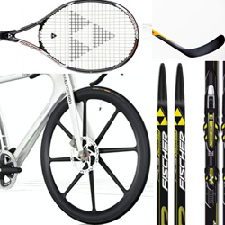
Rice. 2. Bicycle reinforced with nanofibers
Sixth place– plastics reinforced with carbon fibers. Composite materials - light and strong - have transformed many industries: aircraft, space technology, transportation, packaging, sports equipment.
Seventh place– materials for lithium ion batteries. It is hard to imagine that until recently we did without laptops and mobile phones. This "mobile revolution" would not have been possible without the transition from rechargeable batteries using aqueous electrolytes to more energy-intensive lithium ion batteries (cathode - LiCoO__2__ or LiFeO__4__, anode - carbon).
Eighth place– carbon nanotubes (1991), their discovery was preceded by no less sensational discovery in 1985 of C__60__ fullerenes. Today, the amazing, unique and promising properties of carbon nanostructures are at the center of the hottest publications. However, there are still many questions regarding the methods of their mass synthesis with uniform properties, purification methods, and technologies for their inclusion in nanodevices.

Rice. 3. Metamaterial that absorbs electromagnetic radiation
ninth place– materials for soft printed lithography. Lithographic processes occupy a central place in the production of today's microelectronic devices and circuits, storage media and other products, and there is no alternative in the near future. Soft printed lithography uses a resilient polydimethyloxysilane stamp that can be used multiple times. The method can be used on flat, curved and flexible substrates with a resolution of up to 30 nm achieved today.
Materials have always played an important role in the development of civilization. Scientists say that the history of mankind can be described as a change in the materials used. The eras of the history of civilization were named according to the materials: Stone, Bronze and Iron Ages. Perhaps the current era will be called the century of composite materials. In developed countries, materials science is ranked among the top three areas of knowledge along with information technology and biotechnology.
Each branch of technology, as it develops, makes more and more diverse and high demands on materials. For example, structural materials for satellites and spacecraft, in addition to temperature (high and ultra-low temperatures) and thermal cycling resistance, must have tightness in absolute vacuum, resistance to vibration, high accelerations (tens of thousands of times greater than the acceleration of gravity), meteorite bombardment, prolonged exposure to plasma, radiation, weightlessness, etc. Only composite materials consisting of several components with sharply different properties can satisfy such conflicting requirements.
Layered intermetallic composite with increased heat resistance
Superconductive fiber composite

Wear-resistant dispersion-strengthened composite material
The development of nanotechnologies (one of the sections of modern materials science), according to the forecasts of most experts, will determine the face of the 21st century. This is confirmed by the awarding of four Nobel Prizes in chemistry and physics over the past 15 years: for the discovery of new forms of carbon - fullerenes (1996) and graphene (2010), for developments in the field of semiconductor technology and integrated circuits (2000 ), optical semiconductor sensors (2009). Russia is in second place in the world in terms of investment in nanotechnology, second only to the United States (in 2011, investments amounted to about $2 billion). Currently, science is experiencing a real boom in new materials. In this regard, materials scientists are in demand in many industries: in nuclear energy, medicine, oil production, automotive, aviation, space, defense, energy industries, the elite sports industry, research institutes, and innovative companies producing science-intensive products.

Parts and assemblies of the Sukhoi Superjet 100 made of composite materials

Flexible displays based on graphene
Modern sports equipment made of composite materials
Materials scientists are engaged in the development, research and modification of organic and inorganic materials for various purposes; the processes of their production, structure formation, transformation at the stages of production, processing and operation; issues of reliability and efficiency of materials; computer simulation of the behavior of parts and assemblies under various types of loading; provide technical support to various production departments in matters relating to materials for the manufacture of units and components of equipment, participate in the selection and evaluation of potential suppliers of the company.
Graduates of the “Materials Science” direction of VolgGTU are in demand working in large companies and enterprises: OJSC SUAL branch of VgAZ-SUAL, LLC LUKOIL - Volgogradneftepererabotka, OJSC VNIKTIneftekhimoborudovaniye, OJSC Volgogradneftemash, JSC Central Design Bureau Titan, OJSC Neftezavodmontazh ”, JSC VMK Krasny Oktyabr, JSC Volga Pipe Plant, JSC TK Neftekhimgaz, JSC Expertise, LLC Volgogradnefteproekt, JSC Kaustik, LLC Konstanta-2 and many others.
The training of certified bachelors and masters is carried out within the framework of the direction "Materials Science and Technology of Materials" at
Home > DocumentMINISTRY OF EDUCATION AND SCIENCE OF THE RUSSIAN FEDERATION
State educational institution
higher professional education
"Ivanovo State Textile Academy"
Department of Physics and Nanotechnology
| APPROVE Vice Rector for Academic Affairs V.V. Lyubimtsev "_____" ___________________ 2011 |
||
| Materials science of nanomaterials and nanosystems |
||
| Code, direction of preparation | 152200 Nanoengineering |
|
| Training profile | Nanomaterials |
|
| Cycle, code | Mathematical and natural science (B.3.1-3a) |
|
| Semester(s) | ||
| Qualification (degree) of the graduate | bachelor |
|
| Form of study | full-time |
|
| Faculty | fashion industry |
|
Ivanovo 2011
As a result of studying the discipline "Materials Science of Nanomaterials and Nanosystems", students should: know: - properties and applications of nanodispersed powder, fullerene nanostructured solid, liquid and gel-like materials, nanosized elements and objects, nanosystems (heterostructures); fundamentals of nanotechnologies for obtaining nanomaterials; fundamentals of nanotechnologies for obtaining nanostructured and gradient hardening, protective and functional layers and coatings; basics of technological processes for the synthesis of composite materials; be able to: - select nanostructures and methods of their production for the implementation of nano-objects with specified characteristics for the specific requirements of the conversion of electrical, optical, magnetic, thermal and mechanical signals; - use the basic concepts and definitions in the formation of in-depth knowledge in the field of nanoengineering; - analyze the features of nanoproducts and nanotechnologies; draw up diagrams of technological equipment and devices for nanotechnological processes. own: - skills in solving problems of knowledge formation in the field of nanoengineering. The work program of the discipline provides for the following types of educational work:
| Type of study work | Total hours / credits | Semester number |
|
| Classroom activities (total) | |||
| Including: | |||
| Practical classes (seminars) | |||
| Independent work (total) | |||
| Preparation for practical classes (seminars) | |||
| The study of theoretical issues submitted for independent study | |||
| Preparation for the test | |||
| Type of intermediate certification (test, exam) | |||
| Total labor intensity: hours credits | |||
The history of the emergence of nanomaterials, the dynamics of their development and implementation in practice.
Basic concepts and classification of nanostructured materials.
Features of properties and main types of nanoscale systems.
Technological processes of production, processing and modification of nanomaterials and products based on them.
| Department head | A.K. Izgorodin |
| Teacher-developer |
The Department of Nanotechnology, Materials Science and Mechanics was established in December 2011 on the basis of two departments of the TSU Institute of Physics and Technology and has deep historical roots. At the origins of the department were world-class scientists, professors M.A. Krishtal, G.F. Lepin and E.A. Mamontov, who made a huge contribution to the science of physical materials science and created the foundation of the research base for materials science at the university. Section "Mechanics"; base department "Nanomaterials" (Moscow, TsNIIchermet named after I.P. Bardin), scientific and educational center "Physical materials science and nanotechnologies"; More than 20 modern, well-equipped educational and research laboratories for electron, laser, atomic force microscopy, physical and mechanical testing, X-ray diffraction analysis, metallography and acoustic emission, etc., three of which are accredited in the systems of Rostekhnadzor and analytical laboratories (SAAL ); International School "Physical Materials Science" Cooperation with leading Russian and foreign scientific schools, including universities in Germany (Freiberg), Japan (Osako, Kyoto), Australia (Melbourne), etc. All senior students are engaged in fruitful research work and annually become winners and laureates of competitions of scientific works and diploma projects. Almost 100% of the graduates of the department are employed, of which 80% work in their specialty in the research center and laboratory testing department of PJSC AVTOVAZ, laboratories of the Samara Regional Innovation and Technology Center, as well as in expert organizations. Acting Head of Department professor, doctor of technical sciences KlevtsovGennady Vsevolodovich Areas of trainingUndergraduate: Master's degree: (profile "Engineering of advanced materials and diagnostics of the behavior of materials in products") PhD: (profile "Physics of Condensed Matter") – 22.06.01 Technology of materials (profile “Metal science and heat treatment of metals and alloys”) The objectives of the educational program 22.04.01 Materials science and technology (Engineering of advanced materials and diagnostics of the behavior of materials in products): C 1. Preparation of a graduate for research work in the field of modern materials science. C2. Preparation of a graduate for the creation of new materials, the study of their properties, the development of technology for their production. C3. Preparation of a graduate for the design of materials with desired properties. C 4. Preparation of a graduate for production and technological activities, which ensures the introduction into operation of new high-tech developments that are in demand at the world level. DisciplinesTeachers of the department "Nanotechnology, Materials Science and Mechanics" conduct classes in the following disciplines: – Theoretical mechanics; – Strength of materials; – Theory of machines and mechanisms; - Machine parts; - Materials Science; – Technology of structural materials; – Nanotechnologies in production and ecology; – Physical and chemical bases of nanotechnologies; – Materials science of nanomaterials and nanosystems; – Physics of the condensed state; – Phase equilibria and structure formation; – Physical materials science; – Strength of alloys and composites; – New technologies and materials; – Methods for hardening structural materials; – Non-destructive research methods, etc. Did not find an answer to your question? Look at here
|
 Two heads and six legs; four walk, and two lie still
 Self-esteem - what is it: concept, structure, types and levels
 Cassandra's Path, or Pasta Adventures War on Earth and Underground